The need for lower latencies and higher bandwidths has pushed the use of FPGAs into more and more compute applications across many different markets and domains. With this increased demand comes challenges of balancing the performance and economics of FPGA usage, thus driving the need to do more processing with less fabric. This drive to squeeze as much performance out of as few logic gates as possible can be a recipe for disaster if the appropriate architectural and system considerations aren’t addressed early in a new design effort.
In modern FPGA designs, achieving high clock frequencies and wide data paths are often essential to meet complex interface and intensive processing requirements. However, as fabric utilization increases, even meticulously architected designs can struggle to achieve timing closure. This challenge can lead to extended build times, inconsistent performance, and project delays. In this blog, we’ll explore the technical aspects of logic congestion in FPGAs and describe effective strategies for mitigation.
Understanding how performance parameters affect timing closure is critical in synchronous FPGA designs:
– Clock Frequency: In a synchronous design, logic functions, such as Look-Up Tables (LUTs) and multiplexers, receive clocked inputs and drive registered outputs. Typically, a logic function must produce a valid output within a single clock period. As clock frequency increases, the logic resolution time is compressed, potentially causing complex, multi-level logic functions to violate setup time requirements and create critical timing paths.
– Data Bus Width: Widening a data bus enables higher data rates at a given clock frequency but can create fabric utilization and timing challenges. Each additional signal increases resource consumption within the FPGA fabric, introduces unique propagation delays through the fabric, and increases burden on the placement engine to converge on a nominal routing path. This variation in arrival times across the bus, known as bus skew, becomes progressively more problematic for data paths with near-zero slack time. Furthermore, unconstrained bus skew can exhibit considerable variation between synthesis and place-and-route iterations.
Let’s examine an FPGA implementing an 8-lane, 64 GT/s PCI-Express Gen3 interface. To meet bandwidth requirements, the fabric operates at 250 MHz with a 256-bit data bus. Twelve incoming ADC data streams, each averaging 4 Gb/sec, time-division multiplex their access to this interface, with sufficient buffering to support round-robin arbitration.
If this design utilizes approximately 60% of the FPGA fabric, then you might observe significantly lengthened build times due to increased placement and routing effort. Furthermore, timing violations may intermittently appear from build to build, often within the converging data paths of the ADC streams. Inconsistent place and route timing results are often a strong indicator of logic congestion, as the tools struggle to produce an optimal solution within the constrained fabric.
Let’s explore specific techniques that target the root causes of timing violations.
Pipelining for Routing Delay Reduction:
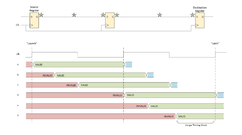
A timed path includes routing and logic elements between the launch (or source) register and the latch (or destination) register. Pipelining involves inserting one or more registers into a timed path to divide it into several separately timed paths. The diagrams below illustrate a simplified example of how pipelining works. The first diagram depicts a prime candidate for pipelining:

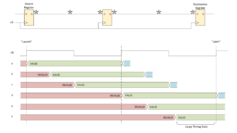
At various points in the path, you can see the propagation delay of the signal launched from the source register. It happens to reach the destination register just in time for the next clock, yielding very little timing slack. By adding a pipeline register in the middle of this path, the timing slack at the destination registers increases dramatically:

This technique is particularly effective when timing violations are dominated by routing delays, indicating a large physical distance between source and destination registers. Routing delays are exacerbated by the addition of combinatorial primitives, such as Look up Tables (LUTs), within the timed path. A well-placed pipeline register can segment such a path, thus reducing the data path length (and its associated propagation delay) and potentially decoupling the physical proximity of related logic functions, thereby decreasing localized congestion.
While straightforward to implement, pipelining introduces latency, delaying data arrival by one clock cycle per pipeline stage. For ultra-low latency designs, this can be a critical factor. Furthermore, careful functional analysis is required to ensure proper synchronization of pipelined data signals or buses at common endpoints, which may necessitate additional data buffers and increase resource utilization and latency.
Simplifying Complex Logic Functions:
When timing violations are generated by logic delays rather than routing delays, simplifying complex logic functions becomes essential. This involves decomposing multi-level asynchronous logic into simpler components that can be pipelined. For instance, the 12-to-1 multiplexer with arbitration logic in our example, exhibiting nine levels of asynchronous logic, could be restructured by implementing a cascade of smaller multiplexers (e.g., three 4-to-1 muxes feeding a 3-to-1 mux), interconnected with pipeline registers.
This approach allows the design to leverage the FPGA fabric’s optimization for fewer inputs. Pipelining the outputs of these smaller stages prevents EDA tools from re-optimizing them into a single complex function, ensuring shorter timing paths and more efficient resource utilization. This approach directly addresses logic-induced timing violations and can alleviate congestion.
Device Selection:
If initial analysis and critical design reviews indicate that the targeted FPGA’s resources are insufficient to meet the design’s performance and density requirements, migrating to a more capable device is a viable strategy.
– Speed Grade Improvement: FPGAs are offered in various speed grades, each with different performance characteristics. Upgrading to a higher speed grade of the same device family can provide modest gains in logic switching characteristics. For example, a Zynq-UltraScale+ MPSoC FPGA might show a 15% performance improvement from speed grade -1 to -2, and a further 10-12% from -2 to -3. While these gains primarily apply to logic cells and less to routing, the cumulative effect on logic delays can be significant for intermittently failing paths.
– Increased Fabric Resources: If high utilization is leading to sub-optimal placement and routing, selecting a pin-compatible or same-family device with a larger fabric can provide the placement and routing tools with more flexibility. This often leads to more ideal placement and simplified routing, addressing congestion directly.
– Newer-Generation FPGA: Migrating to a newer-generation FPGA, often based on smaller fabrication processes, can offer substantial performance improvements across the board, including lower power consumption, faster switching, and enhanced logic structures and routing networks. For instance, the Versal Adaptive SoC family, compared to UltraScale+, features a CLB structure with four times more registers and LUTs and improved support for cascaded multi-level asynchronous logic. While this may require reconfiguring or replacing IP cores, the performance headroom for current and future needs can be significant.
Significant timing closure issues occurred when implementing a custom multi-channel transposed FIR filter on a small FPGA with limited Block RAM and DSP resources. The design required accumulated values to be stored in Block RAM, which were then read (with output registers enabled) and fed directly into DSP blocks for processing.
As development progressed and additional modules were integrated, timing performance began to degrade. Critical path analysis revealed bottlenecks in the direct connections between Block RAM and DSP primitives. The placement constraints of these hardened primitives severely limited the routing options available to the tools.
By strategically inserting pipeline registers between the Block RAM outputs and DSP block inputs, we significantly improved routing flexibility. Along with a modest control logic update to preserve filter throughput, this architectural modification:
– Dramatically enhanced timing performance
– Enabled successful integration of additional design components
– Required minimal additional register resources
– Added only a small, manageable increase to filter latency
This optimization demonstrates how targeted pipelining can overcome inherent physical constraints in FPGA designs when working with fixed primitive locations.
Successfully managing logic congestion in FPGA designs requires a deep understanding of how clocking, data paths, and logic complexity interact with the underlying fabric. Careful architectural planning is essential, but may not always prevent congestion, especially as designs exceed utilization expectations and/or require ultra-high system clock rates. The approaches outlined here, pipelining for routing delay reduction, simplifying complex logic functions, and strategic device selection, provide a robust set of options to overcome congestion-induced timing violations. These strategies apply across various high-clock-rate designs and are vital for achieving robust and reliable embedded systems. If you need support with FPGA development, including complex timing closure challenges like logic congestion, fill out the form below and someone from our team will reach out to discuss how we can help.
Looking to connect with an experienced team?
Look no further than Re:Build AppliedLogix! We are excited to connect with you.